Seriously, Make Your Own Symbols & Footprints
In this post, I’ll highlight the two main problems with using premade symbols and footprints - whether they come from built-in software libraries (like those in Altium Vault or KiCad) or are downloaded from the internet. While it might seem like a time-saver, it’s often much more reliable to create your own. Most datasheets provide detailed and accurate information to help you build correct symbols and footprints with minimal effort.
If you still choose to use premade components, make sure to thoroughly review every symbol and footprint yourself. A quick check now can save you days of debugging and a lot of wasted time and money down the line.
Mistakes in Symbols & Footprints
I hate seeing people use premade symbols or footprints that either come with their electronics CAD tool or were downloaded off the internet. They often have mistakes, and I’ve run into this problem way too many times. I’ve worked on countless designs where someone took a shortcut - instead of putting in the effort to make a proper symbol or footprint, they just grabbed one off the internet. Sure, it’s a time saver... but then we get the board back and it doesn’t work. We end up spending days troubleshooting, only to find out the issue was a faulty premade part - maybe pins were mislabeled, maybe the package was wrong. Suddenly, that “five-minute time saver” has cost us days of work. And the money wasted on boards with a broken part? That adds up fast. If it's a personal project, that’s money straight out of your pocket.
Some people do use these premade components and get away with it. But if your board has a decent number of parts, it’s almost guaranteed that something will go wrong. Maybe not a full failure, but at the very least, something won’t work quite right.
I occasionally look at premade footprints or symbols, usually for weird packages or connectors, just to get a second opinion. And even then, I still find issues fairly often. Many of these parts are autogenerated by software, not manually reviewed. The companies behind them often rely on users to find the mistakes and report them. That’s a pretty bad situation when people are trusting these parts and hoping someone else already caught the errors and reported it.
One of the worst experiences I had was when a senior designer, working under a tight deadline, used a bunch of premade parts from the Altium Vault. When we reviewed them, I think we found issues in nearly every single one. It’s wild - Altium actually uses the Vault as a selling point for their tool, but in my experience, it is terrible. And to be clear, Altium is still my favorite PCB design tool. But I don’t trust the Vault. Honestly, I wouldn’t trust anyone’s premade components.
Footprint Layers
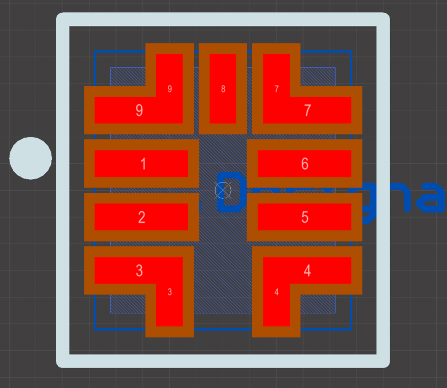
Another important issue that I don’t see mentioned often enough is how inconsistent the layer assignments are in premade footprints. For example, in Altium, the mechanical layer number used for a specific type of information can vary widely between designs. Just because a premade footprint uses Mechanical Layer 3 for the courtyard or dimensions doesn’t mean that matches how your project is set up.
This can lead to a confusing situation when you import these footprints into your PCB layout. You might end up with multiple layers all containing similar or duplicate information, just on different mechanical layer numbers. Altium does have settings that help merge these layers, and it usually does a decent job. But that still depends on the original footprint being set up correctly, which often isn’t the case.
I don’t have as much experience with KiCad, but I would guess it has similar issues when it comes to user-defined layers and imported footprints.
On a related note, people often use different types of layers for different purposes. In my own designs, I try to keep the number of layers to a minimum - only what I actually need. But other designers might include all kinds of additional layers depending on their workflow. When you use a premade footprint, it might come with extra layers you don’t need, or it might be missing ones that you rely on. I’ve seen plenty of designs where the PCB has 30 or more layers, most of them just redundant variations of the same information, scattered across different mechanical layer numbers.
Conclusion
Using premade symbols and footprints is a bad idea. It might be a time saver in the short term, but it could cost you even more time and money later.
